The ever-evolving landscape of semiconductor technology, where minuscule components hold the key to cutting-edge innovations, Probe Cards stand as unsung heroes. These tiny, sophisticated devices play a pivotal role in the production of semiconductors, ensuring that each microscopic element functions flawlessly. Probe Card Manufacturing, we will unravel the intricate process behind their creation, the evolving technologies that drive them, and the indispensable role they play in pushing the boundaries of what is possible in the nanoworld.
What Are Probe Cards?
- Definition and Purpose
Probe Cards, also known as testing or wafer probe cards, are essential tools in the semiconductor manufacturing process. Their primary function is to test the individual integrated circuits (ICs) on a semiconductor wafer. These wafers, typically made of silicon, are the starting point for creating a multitude of electronic devices, from microprocessors to memory chips.
- Structure and Components
Probe Cards consist of a base, often made of ceramic or organic materials, with an array of tiny probes or needles attached. These probes make contact with the pads on the semiconductor wafer, enabling electrical testing of each IC. The precision and density of these probes are crucial, considering the minuscule size of modern semiconductor components.
The Intricate Dance The Manufacturing Process:
- Design and Prototyping
The journey of a Probe Card begins with meticulous design and prototyping. Engineers carefully consider the specifications of the semiconductor devices they will be testing, ensuring that the probe layout aligns with the arrangement of the ICs on the wafer. This phase involves advanced computer-aided design (CAD) tools and simulations to optimize the performance of the probe arrangement.
- Material Selection
The choice of materials is critical in Probe Card Manufacturing. The base material must provide the necessary rigidity, electrical insulation, and thermal stability. Ceramic materials are commonly favored for their excellent thermal properties, while organic materials may be chosen for specific applications. The probes themselves are typically made of materials like tungsten or beryllium copper for their conductivity and mechanical properties.
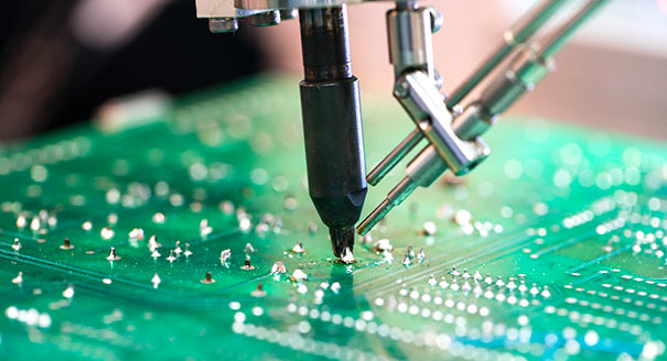
- Precision Machining
Once the design is finalized and materials are selected, the manufacturing process moves to precision machining. Advanced machining techniques, such as electrical discharge machining (EDM) and laser micromachining, are employed to carve out the intricate patterns for the probes and the overall structure of the card. The level of precision required at this stage is on the scale of micrometers, highlighting the extraordinary precision demanded by the nanoworld.
- Assembly and Testing
The assembly of a Probe Card involves affixing the probes to the base, ensuring they are correctly aligned with the designed layout. This delicate process demands a sterile environment to prevent any contaminants that could compromise the performance of the probes. After assembly, each Probe Card undergoes rigorous testing to verify the functionality and alignment of the probes. Any deviations could result in inaccurate testing of the semiconductor devices.
Evolving Technologies Pushing the Boundaries:
- Microfabrication Techniques
As semiconductor technology continues to advance, so do the techniques employed in Probe Card Manufacturing. Microfabrication technologies, borrowed from the semiconductor industry itself, enable the creation of smaller, more densely packed probes. This allows for testing the ever-shrinking components of modern semiconductor devices with unparalleled precision.
- MEMS Technology
Microelectromechanical systems (MEMS) technology has also found its way into Probe Card Manufacturing. MEMS-based probes, with their tiny movable structures, offer enhanced flexibility and contact accuracy. They can adapt to the varying heights of the ICs on a wafer, ensuring reliable contact during testing. This integration of MEMS technology represents a leap forward in the quest for higher testing accuracy and efficiency.
- Advanced Materials
The choice of materials for Probe Cards continues to evolve. Researchers are exploring new materials with superior electrical properties, enhanced durability, and thermal stability. Nanomaterials, with their unique properties at the nanoscale, are under consideration for future Probe Card designs, promising even higher performance and reliability.
The Crucial Role of Probe Cards in Semiconductor Manufacturing:
- Quality Control
Probe Cards are at the forefront of ensuring the quality and reliability of semiconductor devices. By thoroughly testing each IC on a wafer before it is separated and packaged, manufacturers can identify and address any defects early in the production process. This is crucial for meeting the demanding quality standards of the semiconductor industry.
- Yield Enhancement
In semiconductor manufacturing, yield is a critical metric that measures the percentage of usable ICs on a wafer. Probe Cards directly impact yield by detecting and eliminating faulty components. The more accurate and efficient the testing process, the higher the yield, leading to lower production costs and increased profitability.
- Time and Cost Efficiency
The speed and efficiency of semiconductor testing directly influence the overall manufacturing timeline and cost. Probe Cards play a pivotal role in accelerating the testing phase, ensuring that the vast number of ICs on a wafer are teste swiftly and accurately. This efficiency is paramount in meeting the demands of a fast-paced industry where time-to-market can make or break a product.
Conclusion:
As we delve into the intricate world of Probe Card Manufacturers, it becomes evident that these tiny devices wield immense influence over the capabilities of the semiconductor industry. The constant push for smaller, more powerful semiconductor components necessitates a parallel advancement in the technologies used to test them. From precision machining to the integration of cutting-edge technologies like MEMS, Probe Card Manufacturing stands as a testament to the relentless pursuit of innovation in the nanoworld.